Sony Exmor RS sensors to allow slimmer, better camera phones
posted Monday, August 20, 2012 at 2:29 PM EDT
 Early this year, Sony revealed that it was working on a new generation of backside-illuminated image sensors that would move more of the peripheral circuitry at each photodiode location beneath the active pixels, replacing the supporting substrate in the process.
The design can be used to reduce the overall sensor area while maintaining the same photodiode area, translating to a smaller overall imaging module size. Alternatively, the sensor size can be retained while increasing the light gathering area, and thereby improving the sensitivity and noise characteristics. Given the push for ever-thinner phones with better camera quality, both benefits are likely of great import to smartphone manufacturers. (Of course, a middle ground can be achieved by reducing the sensor size somewhat while still increasing the pixel size.)
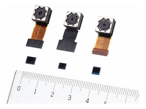
At the time, no date was given for the sensors to be commercialized, although the company predicted that the new chips would be available for sampling from the middle of the year. Now, Sony has announced launch dates for three CMOS image sensors featuring the technology, each of which will share new Exmor RS branding. As well as the bare chips, Sony will also provide a prepackaged imaging module based around each sensor.

Photo provided by Sony Corp.
First to arrive will be the 1/4-inch type, Sony ISX014 image sensor, with 8.08 megapixel effective resolution and a diagonal of about 4.6mm. The sensor has a standard RGBG Bayer filter, and a readout rate of 15 frames per second at full resolution, 30 fps when 1/2 sub sampled, and a whopping 120 fps when 1/8 sub sampled. Movie modes will include 30 fps Full HD (1,920 x 1,080 pixels), and 60 fps 720p (1,280 x 720 pixels).
Shipping as a bare sensor from October 2012, the ISX014 will also be integrated into the IUS014F-Z module the following month. The 4.65mm-deep module will feature an all-plastic, four element lens with a fixed f/2.4 aperture and 28mm-equivalent focal length. Autofocus is catered for with a voice coil motor. Sensor-only sample pricing is ¥1,200 (US$15), while the full module with autofocus lens samples for ¥6,000 (US$75).
Next up is the 1/3.06-inch Sony IMX135 image sensor, with 13.13 megapixel effective resolution and a diagonal of about 5.9mm. This larger sensor swaps in an RGBW pixel structure for increased sensitivity at the expense of some color resolution, but still yields standard Bayer raw output, so that it can be plugged into an existing RGBG pipeline. It offers a readout rate of 24 frames per second at full resolution, and 48 fps when sub sampled to half resolution. As described last spring, it includes an unusual HDR movie mode that allows sampling of some pixels while exposure continues for others. This HDR mode will be possible only at 30 fps Full HD (1,920 x 1,080 pixel) resolution. For normal, non-HDR imaging, rates of 60 fps will be possible for both Full HD and 720p capture.
Shipping as a bare sensor from January 2013, the IMX135 will also be integrated into the IU135F3-Z module from March 2013. Thanks to the larger sensor size, the module is also a bit deeper, at 5.5mm. It still features an all-plastic, 28mm, VCM autofocus lens, but with five elements and a brighter fixed f/2.2 aperture Sensor-only sample pricing is ¥1,500 (US$20), and the module samples for ¥8,000 (US$100).


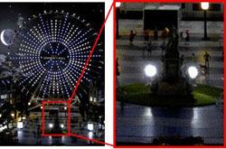
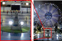
Images courtesy of Sony Corp.
Finally, the IMX134 image sensor and IU134F9-Z module will follow from March and May 2013 respectively. The IMX134 sensor is very similar to the standard Bayer chip, with a 1/4-inch form factor and 8.08 effective megapixel resolution. It integrates the RGBW filtering of the IMX135, though, as well as the HDR movie functionality, although this runs only at a lower resolution of 720p with 30 fps rate. Although its module is similar to that used for the Bayer-filtered sensor, it's actually the slimmest of the trio, at 4.2mm. This chip has the lowest sample pricing, at ¥1,000 (US$13) bare, and ¥5,000 (US$63) for the module.
Note: All US dollar prices in this article are approximations based on conversion at current exchange rates, and do not take into account fluctuations in currency value, exchange rates, duties, and the like.
Press Release
Sony Develops “Exmor RS,” the World's First*1 Stacked CMOS Image Sensor
Also introduces imaging modules that deliver high picture quality and compact size, for use in mobile devices such as smartphones and tablets
- Sony Continues to Advance the Evolution of World of Digital Imaging -
*1 As of August 20, 2012
August 20, 2012, Tokyo, Japan - Sony Corporation (“Sony”) today announced the commercialization of “Exmor RS,” the world's first(*1) CMOS image sensor incorporating a unique, newly-developed ‘stacked structure.’ Shipments will commence in October. Sony is introducing three models of the “Exmor RS,” stacked CMOS image sensor, for use in smartphones and tablets, which combine superior image quality and advanced functionality with compact size. Sony will also launch three corresponding imaging modules incorporating these sensors.
Going forward, Sony will continue to evolve its digital imaging products, while aggressively pursuing the further development and expansion of its core “Exmor RS” stacked CMOS image sensor technologies and lineup, in order to deliver increasingly diverse and user-friendly image capturing experiences.
Two of the three “Exmor RS” models Sony is launching are the ‘IMX135’, a type 1/3.06 model with 13.13 effective megapixels and the ‘IMX134’, a type 1/4 model with 8.08 effective megapixels, which feature ‘RGBW coding’ function and ‘HDR (High Dynamic Range) movie’ function. The ‘RGBW coding’ function can capture sharp, clear images even when filmed or photographed in low light conditions, such as a dark room or at night by featuring W (white) pixels in addition to conventional RGB (red-green-blue) pixels, and leveraging Sony’s proprietary device technology and signal processing to heighten sensitivity without compromising its high resolution. ‘HDR (High Dynamic Range) movie’ function enables two different exposure conditions to be configured within a single screen when shooting, and seamlessly performs appropriate image processing to generate optimal images with a wide dynamic range and brilliant colors, even when pictures are taken against bright light. The other “Exmor RS” model is the ‘ISX014’, a type 1/4 model with 8.08 effective megapixels, which has a built-in camera signal processing function.
In addition to the higher image quality and superior functionality, the use of a ‘stacked structure’ has helped Sony to achieve a more compact size.
Sony will also bring to market three compact auto-focus imaging modules equipped with lens units and featuring auto-focus mechanisms that incorporate these image sensors: the ‘IU135F3-Z,’ ‘IU134F9-Z’ and ‘IUS014F-Z’. These three imaging modules adopt a newly-designed lens which has been optimized for the industry’s smallest(*1) 1.12μm unit pixel size to achieve higher resolution.
The ‘IU135F3-Z’ is an auto-focus imaging module incorporating a bright, high-resolution F2.2 lens. The ‘IU134F9-Z’ (W:8.5 x D:8.5 x H:4.2mm(*4)) is thin and compact. The ‘IUS014F-Z’ is an all-in-one imaging module that comprises an image sensor with built-in camera signal processing function and built-in auto-focus and picture adjustment function.
Going forward, Sony plans to continue with the proactive development of its “Exmor RS” stacked CMOS image sensors in order to bring to market imaging modules that achieve higher image quality, advanced functionality and an even more compact size. Sony aims to leverage the characteristics of its ‘stacked structure’ design to respond to the demand for larger screens in devices such as smartphones, where the amount of space available for embedding imaging modules is limited, and to continue expanding its product lineup to better accommodate its customers’ needs.
Demand is growing rapidly for mobile devices such as smartphones and tablets, and Sony is committed to strengthening its production capacity(*2) for stacked CMOS image sensors, which combine the dual strengths of advanced functionality and compact size. This will enable Sony to solidify its position as the global leader in CMOS image sensors, and to act as a driving force for the industry in the future.
*2: An announcement was already made (on June 22) regarding capital investment at Sony Semiconductor Corporation's Nagasaki Technology Center with the objective of increasing the production capacity for stacked CMOS image sensors.
| Model |
Shipment date (planned) |
Sample price (incl. tax) |
|
|
Type 1/3.06 13.13 effective megapixels(*3) |
Stacked CMOS image sensor 'IMX135' |
January, 2013 | 1,500 JPY |
|
Imaging module 'IU135F3-Z' |
March, 2013 | 8,000 JPY | |
|
Type 1/4 8.08 effective megapixels(*3) |
Stacked CMOS image sensor 'IMX134' |
March, 2013 | 1,000 JPY |
|
Imaging module 'IU134F9-Z' |
May, 2013 | 5,000 JPY | |
|
Type 1/4 8.08 effective megapixels(*3) |
Stacked CMOS image sensor 'ISX014' |
October, 2012 | 1,200 JPY |
|
Imaging module 'IUS014F-Z' |
November, 2012 | 6,000 JPY | |
*3: Based on the method for specifying effective pixels in image sensors
Main Features
"Exmor RS" stacked CMOS image sensor
-
Commercialization of new, independently-developed "Exmor RS," incorporating the world's first(*1) unique 'stacked structure'
-
This stacked structure facilitates higher image quality, advanced functionality and a more compact size.
-
Equipped with 'RGBW coding' and 'HDR movie' functions ("IMX135" and "IMX134")
-
Equipped with a built-in camera signal processing function, enabling compatibility with automatic controls, picture adjustment and multiple image output formats (such as YUV) ("ISX014")
-
Main Features
Imaging modules(each image sensor is mounted with a built-in lens unit with auto-focus mechanism)
-
High resolution has been achieved by adopting a newly-designed lens, which is optimized for the industry's smallest(*1) 1.12μm unit pixel size.
-
The "IU135F3-Z" auto-focus lens module adopts a bright F2.2 high-resolution lens.
-
The "IU134F9-Z" achieves a thin, compact size (W:8.5 x D:8.5 x H:4.2mm(*4)).
-
The "IUS014F-Z" is an all-in-one model capable of picture adjustment that comes equipped with a camera signal processing function.
Key specifications
Stacked CMOS image sensors
| Model name | IMX135 | IMX134 | ISX014 | |
| Number of effective pixels |
4208(H) x 3120(V) 13.13M pixels |
3280(H) x 2464(V) 8.08M pixels |
3280 (H) x 2464 (V) 8.08M pixels |
|
| Image size |
Diagonal 5.867 mm (Type 1/3.06) |
Diagonal 4.595 mm (Type 1/4) |
Diagonal 4.6 mm (Type 1/4) |
|
| Unit cell size | 1.12 μm (H) x 1.12 μm (V) | 1.12 μm (H) x 1.12 μm (V) | 1.12 μm (H) x 1.12 μm (V) | |
| Frame rate | Full | 24 fps | 30 fps | 15 fps |
| 1/2 sub sampling | 48 fps | 60 fps | 30 fps | |
| 1/8 sub sampling | Not supported | Not supported | 120 fps | |
| HD mode |
1080p 30fps (HDR mode) 1080p 60fps 720p 60fps |
1080p 30fps 720p 30fps (HDR mode) 720p 60fps |
1080p 30fps 720p 60fps |
|
|
Sensitivity (typical value F5.6) |
92mV (Green pixel) 127mV (White pixel) |
92mV (Green pixel) 127mV (White pixel) |
84mV | |
|
Sensor saturation signal (minimum value) |
260mV | 260mV | 260mV | |
|
Power supply |
Analog | 2.7V | 2.7V | 2.7V |
| Digital | 1.05V | 1.05V | 1.05V | |
| Interface | 1.8V | 1.8V | 1.8V, 2.7V | |
| Key features |
RGBW coding function HDR movie function |
Auto-control function Picture quality adjustment function |
||
| Output | MIPI (4lane, 2lane) | MIPI (4lane, 2lane) | MIPI (4lane, 2lane, 1lane) | |
| Image output format | Bayer RAW | Bayer RAW |
YUV,RGB,RAW, Y/Cb/Cr, JPEG + YUV (thumbnail), JPEG (4:2:2) |
|
Key specifications
Imaging module
| Model | IU135F3-Z | IU134F9-Z | IUS014F-Z |
| Module size(*4) | W:8.5 x D:8.5 x H:5.5 mm | W:8.5 x D:8.5 x H:4.2 mm | W:8.5 x D:8.5 x H:4.65 mm |
| AF actuator | VCM (Voice Coil motor) | ||
| Lens composition |
Plastic (5 groups 5 elements) |
Plastic (4 groups 4 elements) |
Plastic (4 groups 4 elements) |
| F-number | F2.2 | F2.4 | F2.4 |
|
Focal length (35mm conversion) |
28mm | ||
*1: Accurate at time of press release (August 20, 2012)
*2: An announcement has already been made (on June 22) regarding capital investment at Sony Semiconductor Corporation's Nagasaki Technology Center with the objective of increasing the production capacity for stacked CMOS image sensors.
*3: Based on method for specifying effective pixels in image sensors
*4: The dimensions width (W) and depth (D) exclude flexible printed circuits. Typical values exclude tolerance.


