What’s the story with Fujifilm’s X-Trans sensor tech? Is it really all that different?
posted Monday, April 20, 2020 at 4:30 PM EDT

More than perhaps any other company, Fujifilm has a long history as an innovator in image sensor design. From the very beginning of the digicam boom, its rivals have almost exclusively used standard, Bayer-filtered sensors in their standalone cameras. Fuji, though, hasn't been afraid to buck that trend in its quest for better image quality.
Super CCD technology led the way for what was to come
In the early 2000s, Fujifilm went its own way with its Super CCD technology, first seen in the FinePix 4700, announced in March of 2000. The Super CCD used an unusual grid of octagonal photosites, rotated at 45 degrees to put its peak resolution on the horizontal and vertical axes, where it would make the biggest difference in real-world shots. And in 2003, the Super CCD SR chip in the FinePix F700 put two photodiodes -- one larger and one smaller -- under each microlens, allowing for increased dynamic range. A subsequent SR II generation for 2005's FinePix S3 Pro put the smaller photodiodes in the gaps between the larger ones, and gave them their own microlenses.
In 2009, the FinePix F200EXR debuted the Super CCD EXR image sensor, which had a newly-designed color filter array that allowed for easier pixel binning, and the ability to clock information off the sensor midway through the exposure for half of its pixels. Together, these allowed it to prioritize resolution, sensitivity or dynamic range as needed for any given shot.

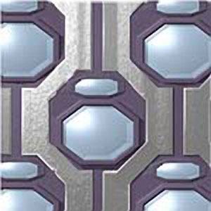

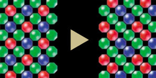
As for the intermediate Super CCD EXR (2009, below), it had a structure akin to that of the original Super CCD, but changed the layout of the red, green and blue pixels making up its Color Filter Array from that seen on the left to that seen at image right.
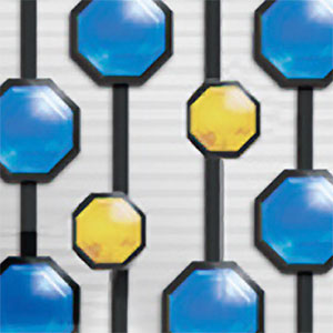
And finally, in 2010, the Super CCD EXR II sensor used in both the FinePix F300EXR and Z800EXR added on-chip phase-detection pixels for faster autofocus -- shown in yellow in the second image above -- an industry first that was eventually adopted by almost all camera manufacturers, and which made the mirrorless camera revolution possible. The Super CCD EXR II also marked the final iteration of the distinctive Super CCD sensor layout, with the resolution of image sensors by then having soared to the point where the increased horizontal and vertical resolution it provided made less of a difference.
Sharper images and less moiré thanks to Fujifilm X-Trans
But while Super CCD faded from memory, it was far from the end of Fujifilm's image sensor innovation. In its place, the first X-Trans image sensor arrived in 2012 with the Fuji X-Pro1. Fujifilm's X-Trans sensor technology followed the idea of using a unique color filter array, but took it much further and in an entirely new direction.
I've mentioned color filter arrays twice now, without describing what they are. At their core, image sensors are like black and white film: They only see a range of brighter or darker tones, with no color information attached. To let them detect color, an array of tiny red, green and blue filters are essentially painted onto the chip, so each sensor pixel will only respond to one of those primary colors. It's as if you had three cameras, each capturing monochrome red, green and blue images that were then combined together to produce a full-color result.


There are two problems with this approach. First, the camera has to do some number-crunching to turn each of the separate red green and blue pixels into full-color RGB ones. This isn't terribly difficult with conventional sensors, but a bigger issue is that the regularly repeating patterns of colored pixels can result in moiré patterns when the subject contains finely-detailed, repeating patterns. (Think of texture in cloth or subjects like venetian blinds.) If you've ever held two pieces of window screen at an angle to each other, you'll have seen the broad swirls of light and dark the conflicting patterns create. The same thing can happen in your camera when a pattern on the subject happens to align in just the wrong way with the regular array of colored pixels on the sensor.
The classic way of dealing with this is to put what's called an optical low-pass filter in front of the sensor. This basically produces a very controlled blurring of the image, so sharp edges and abrupt color and tonal transitions in the subject won't cause problems by interacting with the pixel pattern. Rounding off those sharp edges in the image makes the moiré problem go away, but at the expense of a much softer-looking image.
There's really no way around this; it's a mathematical fact of life, despite what non-mathematicians might tell you. No amount of processing or fancy algorithms can guarantee to eliminate moiré in all cases, if the subject detail is too fine relative to the pitch of the pixels.

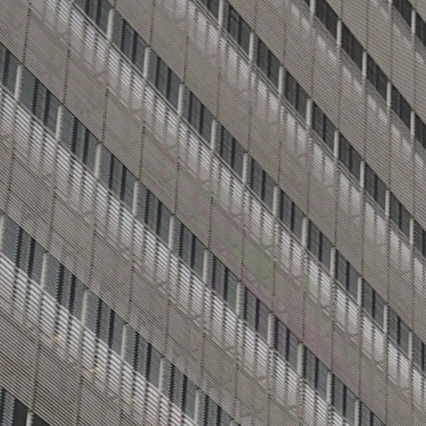
Most cameras these days have dispensed with low-pass filters, getting away without them thanks to sensor resolution outstripping the resolving power of many lenses. In many cases, the lens can't resolve detail fine enough to cause a problem with moiré, so it's basically acting as the low-pass filter in the system relative to the fine pitch of the pixels. With the lens blurring the finest subject detail, the camera doesn't need its own low-pass filter to blur it further.
Of course, you can see the problem with this: What happens if your lens can resolve such fine detail?
It's as much art as science to design a lens that not only has good optical characteristics, but that can also be manufactured reliably and repeatably. Any manufacturing process is a game of managing tolerances, balancing what you'd like to do in an ideal world and what you can actually achieve on the factory floor. This is even more true of lens manufacturing than other types. One way lens designers hedge their bets is to design lenses such that there isn't a single point of absolute best focus, but rather a range over which the focus is more or less the same.
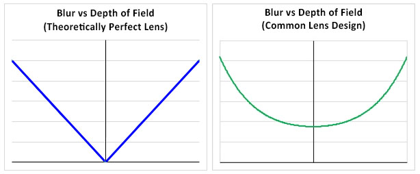
An ideal depth of field curve for a textbook-perfect lens and a sensor of infinite resolution would be a V-shape. In the real world, most lenses are designed to have a flattened bottom on the V, which helps accommodate minor variations in part tolerances during manufacturing.
It was probably six or seven years ago that I had a fascinating sit-down with some of Fujifilm's top optical designers who explained this to me. The point of the conversation was that they'd adopted a different philosophy, aiming for maximum sharpness no matter what, making the point of the "V" as sharp as possible. This means crisper images, but what about moiré?
To some extent, the better your lens is, the more likely you are to see moiré in images of subjects with repeating patterns in them. Part of the reason Fuji felt free to pursue this approach was that they already had a solution in mind, in the form of their X-Trans sensor technology.
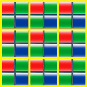
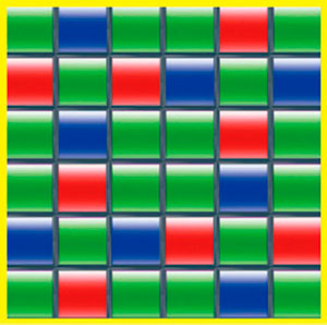
X-Trans changes things up by using a more complex array of color filters. Rather than the two-by-two RGBG Bayer pattern used by most cameras, X-Trans uses a much larger six-by-six array that mixes up the pixel spacing. Depending on where and in what direction you're looking, the spacing between pixels of a given color can vary quite a bit. This gives the camera's image processor more spatial information to help it sort out what's moiré and what's subject detail.
Of course, X-Trans does still have a repeating pattern of colored pixels, so there's not a 100% guarantee that you'll never see a moiré pattern. The bottom line, though, is that X-Trans sensors give the camera a much broader range of spatial frequency information, so its X-processor has more data to use in striking the best balance between moiré and maximized sharpness. It takes a lot of number-crunching (see below), but the different spatial sampling frequencies give the processor more information to work with.
After years of development, X-Trans has truly reached maturity
Like Super CCD before it, Fujifilm's X-Trans sensor technology has continued to evolve over the decade or so since its launch. Since that first generation arrived with the X-Pro1 in 2012, three subsequent generations have refined and extended the technology.
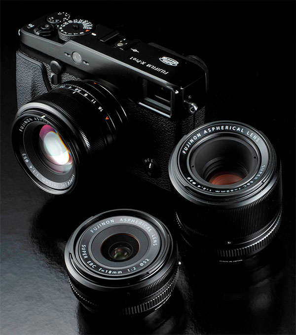
The first X-Trans II chip debuted in the Fuji X100S in 2013. Harkening back to the Super CCD EXR II design that preceded it, Fuji's X-Trans II sensors added on-chip phase-detection autofocus. Improved pixel circuitry also brought better dark-noise suppression, and the resolution jumped from 12.3 to 16.3 megapixels, as well.
In 2016, the third generation X-Trans III arrived with Fuji's X-Pro2. It brought still higher 24.3-megapixel resolution, even more phase-detection AF points, and switched from aluminum to copper wiring, simultaneously lowering noise levels and significantly improving readout speeds and thus camera performance. Most recently of all, the Fujifilm X-Trans CMOS 4 sensor arrived in 2018 with the X-T3. This latest generation switched to a backside-illuminated design for even better light gathering capability, and once again boosted the on-chip phase detection pixel count significantly for more capable autofocus. It also increased the resolution a bit, to 26.1 megapixels. (Click here to read more about Fuji's advanced AF technology, in my executive interview from the 2019 CP+ trade show.)
X-Trans technology is fundamental to Fujifilm's strategy. They view image quality as a key differentiator for their cameras and have invested a huge amount in developing their own sensor technologies in pursuit of it. X-Trans is just the latest iteration in that process, one that was planned years before the processor technology would arrive to make it feasible.
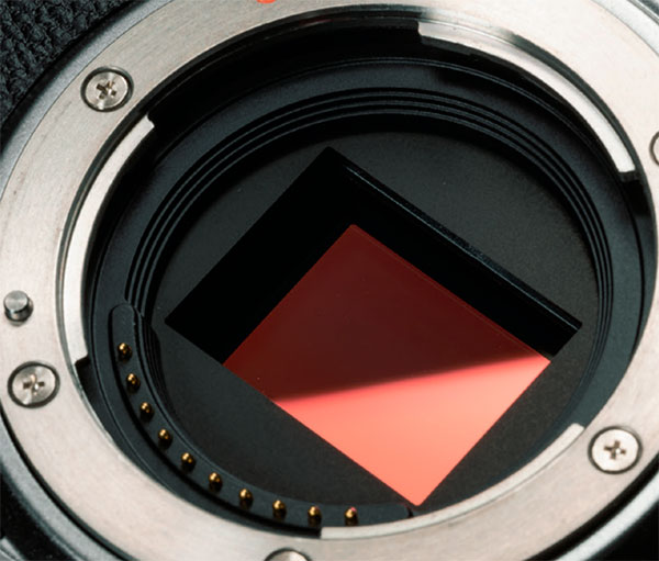
Planning for a future they knew was coming...
Their future planning was one of the things I found most interesting when I interviewed Fujifilm engineers back when X-Trans first appeared. Back in 2012, when the first X-Trans camera debuted, they told me that they had already been working on X-Trans for five or six years by that point. Why did it take so long? Demosaicing data from the X-Trans color filter array to create full-color images in-camera required a lot of processing power, a lot more than was available from in-camera image processors at the time. It took the intervening five years or so for the processor technology to catch up.
They knew that faster processors were coming, though; it wasn't hard to draw a line through a chart of processor power over time and project that there would eventually be image processors that were up to the task. So rather than shelving the idea, they kept working on the concept.
This was fascinating to me. I imagine it's commonplace for companies to make strategic decisions based on where the technology will be in the future, but this was the first time I'd heard a camera company say that their development work was so concretely based on that long a look-ahead. It also influenced their lens designs from an early point, aiming for a future they knew was coming.

More than "just" clever sensor design
These days, improvements in embedded processing mean there's power to spare. In fact, when the first X-Trans CMOS 4 camera arrived some 18 months prior to my writing this, its debut also brought the company's first X-Processor 4 chip, sporting a mobile quad-core design. That was enough power not just for demosaicing X-Trans color filtered images at high resolution and with far more phase-detection AF pixels to boot, it also allowed the company to double its sampling rate for more reliable autofocus and autoexposure, and to add support for 4K video capture as well.
Of course, Fujifilm also had to get software companies like Adobe on board, too, so its customers could process their raw images in their chosen imaging apps. That, too, took some time to achieve, but nowadays raw X-Trans images are well supported by apps like Adobe Photoshop and Lightroom, Phase One's Capture One and more, not just in Fuji's own software. And that's happened because Fujifilm has gone out of its way to foster that development, offering support to the software makers and not charging licensing fees for use of its technology.
The X-Trans based Fujifilm X-T3 was our 2018 Camera of the Year
But all that effort has clearly paid off for the company. When we reviewed the X-Trans CMOS 4-based X-T3, we concluded that it was a "very impressive, very well-rounded camera for both photos and video" offering "serious image quality and performance", and said it was "an excellent camera for sports, wildlife and all manner of subjects". In fact, we were so impressed with the X-T3 and Fuji's X-Trans tech, we also named it our overall Camera of the Year in 2018.

So what's next for Fuji and its image sensor development? I don't know yet -- and of course, even if I did, I couldn't tell you ;-) Based on past history, though, it's a safe bet that the company has already been working on the next big thing for years now. In the meantime, Fujifilm's X-Trans technology has truly come into its own. It offers a genuinely unique approach to image quality, and its advanced autofocus architecture combined with the power of their latest X-processors delivers excellent AF performance as well.
I always like to see companies innovating, and looking off the beaten path for ways to advance the art of photography. I like it even more when those efforts are as successful as Fujifilm's X-Trans sensor tech.
I've wanted to write more deeply about Fuji's X-Trans technology for a long while now, but could never manage it, amongst all the demands on my time from running IR. Thanks to Fujifilm for finally making it possible, through their sponsorship of this article!
